Top Qs
Timeline
Chat
Perspective
Apple A12
System-on-a-chip designed by Apple Inc From Wikipedia, the free encyclopedia
Remove ads
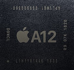
The Apple A12 Bionic is a 64-bit ARM-based system on a chip (SoC) designed by Apple Inc., part of the Apple silicon series,[8] It first appeared in the iPhone XS and XS Max, iPhone XR, iPad Air (3rd generation), iPad Mini (5th generation), iPad (8th generation) and Apple TV 4K (2nd generation).[8][5] Apple states that the two high-performance cores are 15% faster and 40% more energy-efficient than the Apple A11's, and the four high-efficiency cores use 50% less power than the A11's.[8][7] It is the first mass-market system on a chip to be built using the 7 nm process.[9] Updates for the 8th generation iPad, 3rd generation iPad Air, 5th generation iPad Mini and the 3rd generation iPad Pro will still be supported.
Remove ads
Design
Summarize
Perspective
The Apple A12 SoC features an Apple-designed 64-bit ARMv8.3-A six-core CPU, with two high-performance cores called Vortex, running at 2.49 GHz, and four energy-efficient cores called Tempest.[4][5] The Vortex cores are a 7-wide decode out-of-order superscalar design, while the Tempest cores are a 3-wide decode out-of-order superscalar design. Like the A11's Mistral cores, the Tempest cores are based on Apple's Swift cores from the Apple A6.[10]
The A12 also integrates an Apple-designed four-core graphics processing unit (GPU) with 50% faster graphics performance than the A11.[4][8] The A12 includes dedicated neural network hardware that Apple calls a "Next-generation Neural Engine."[11] This neural network hardware has eight cores[7] and can perform up to 5 trillion 8-bit operations per second.[4][5] Unlike the A11's Neural Engine, third-party apps can access the A12's Neural Engine.[12]
The A12 is manufactured by TSMC[1] using a 7 nm[5] FinFET process, the first to ship in a consumer product,[4][1] containing 6.9 billion transistors.[1] The die size of the A12 is 83.27 mm2, 5% smaller than the A11.[13] It is manufactured in a package on package (PoP) together with 4 GiB of LPDDR4X memory in the iPhone XS[2] and XS Max[13] and 3 GB of LPDDR4X memory in the iPhone XR, the iPad Air (2019), the 5th generation iPad mini, and the iPad (2020).[14] The ARMv8.3 instruction set it supports brings a significant security improvement in the form of pointer authentication, which mitigates exploitation techniques such as those involving memory corruption, Jump-Oriented-Programming, and Return-Oriented-Programming.[15]
The A12 has video codec encoding support for HEVC and H.264. It has decoding support for HEVC, H.264, MPEG‑4 Part 2, and Motion JPEG.[16]
Remove ads
Products that include the Apple A12 Bionic
See also
- Apple silicon, the range of ARM-based processors designed by Apple
- Apple A12X
- Comparison of Armv8-A processors
References
Wikiwand - on
Seamless Wikipedia browsing. On steroids.
Remove ads

