Top Qs
Timeline
Chat
Perspective
SEEC microscopy
Optical quantitative imaging technique From Wikipedia, the free encyclopedia
Remove ads
Surface-enhanced ellipsometric contrast microscopy (SEEC) uses an upright or inverted optical microscope in a crossed polarization configuration and specific supporting plates called surfs on which the sample is deposited for observation.[1] It is described as an optical nanoscopy technique.
This article has multiple issues. Please help improve it or discuss these issues on the talk page. (Learn how and when to remove these messages)
|

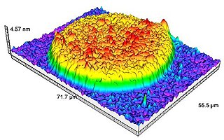
SEEC relies on precise control of the reflection properties of polarized light on a surface, improving the axial sensitivity of an optical microscope by two orders of magnitude without reducing its lateral resolution.[1] Applications could include real-time visualization of films as thin as 0.3 micrometers and isolated nano-objects in air and in water.
Remove ads
Principles
Summarize
Perspective
This section includes a list of references, related reading, or external links, but its sources remain unclear because it lacks inline citations. (February 2024) |


A 2006 study on polarized light coherence led to the development of new supports (the surfs) having contrast amplification properties for standard optical microscopy in cross-polarizer mode.[2] Made of optical layers on an opaque or transparent substrate, these supports do not modify the light polarization after reflection even if the numerical aperture of the incident source is significant. This property is modified when a sample is present on a surf; a non-null light component is then detected after it has been analyzed, rendering the sample visible.
The performance of these supports is evaluated by measuring the contrast (C) of the sample defined as: C = (I1-I0)/(I0+I1) where I0 and I1 represent the intensities reflected by the bare surf and by the analyzed sample on the surf, respectively. For a one nanometer-film thickness, the surfs display a contrast 200 times higher than on silicon wafer.
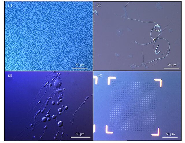
This high contrast increase allows the visualization with standard optical microscope of films with thicknesses down to 0.3 nanometers, as well as nano-objects (down to a 2 nanometer diameter) and this, without any kind of sample labeling (neither fluorescence, nor a radioactive marker). An illustration of the contrast enhancement is in the Figure for optical microscopy between cross polarizers of a Langmuir-Blodgett structure on a silicon wafer and on a surf.
Remove ads
Applications

Life sciences
Thin films and surface treatment
Nano-materials
Commercial applications
Nanolane's Sarfus Mapping Station is based on surface-enhanced ellipsometric contrast microscopy.[10]
References
Wikiwand - on
Seamless Wikipedia browsing. On steroids.
Remove ads
