Top Qs
Timeline
Chat
Perspective
Teardrop (electronics)
Printed circuit board feature From Wikipedia, the free encyclopedia
Remove ads
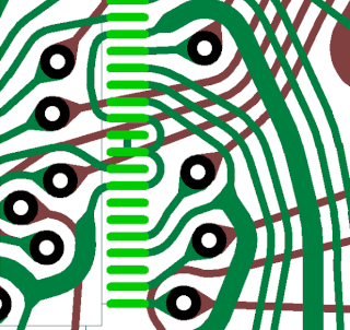
A teardrop is typically drop-shaped feature on a printed circuit board and can be found on the junction of vias or contact pads.

Teardrop vias on printed circuit boards
Purpose
The main purpose of teardrops is to enhance structural integrity in presence of thermal or mechanical stresses,[1][2][3] for example due to vibration or flexing.[4] Structural integrity may be compromised, e.g., by misalignment during drilling, so that too much copper may be removed by the drill hole in the area where a trace connects to the pad or via.[2][3][5] An extra advantage is the enlarging of manufacturing tolerances, making manufacturing easier and cheaper.[3]
Remove ads
Shape
While a typical shape of a teardrop is straight-line tapering, they may be concave.[2] This type of teardrop is also called filleting or straight.[3] To produce a snowman-shaped teardrop, a secondary pad of smaller size is added at the junction overlapping with the primary pad (hence the nickname).[3][6]
Necking
For similar reasons, a technique called trace necking reduces (or necks down[7][8][9]) the width of a trace that approaches a narrower pad of a surface-mounted device or a through-hole with a diameter that is less than the width of the trace, or when the trace passes through bottlenecks (for example, between the pads of a component).[8][9][10][11]
References
External links
Wikiwand - on
Seamless Wikipedia browsing. On steroids.
Remove ads


